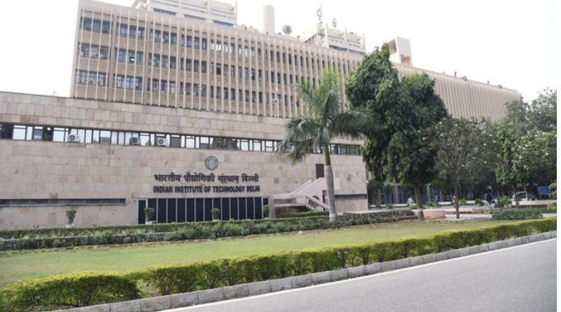
IIT Delhi and BTPL Sign MoU to Develop Diamond-Based Deep UV Photodetectors.
Photo Credit: The Suncity News

New Delhi, October 14, 2024: IIT Delhi and M/s Bhathwari Technologies Pvt. Ltd (BTPL), Surat, a leading company in the area of synthesis of diamonds using Chemical Vapour Deposition (CVD) technique, has signed an MoU for the development of diamond-based deep ultraviolet (UV) photodetectors for the first time in India.
The deep UV photodetectors find applications in the area of UV imaging, secure communication, biological detection, military detection, etc.
The advantages of these photodetectors are their highly selective photo response in the deep UV region and high efficiency at room temperature (RT) and even at higher temperatures.
An IIT Delhi researcher designed the UV Photodetectors:
Under this collaborative work, BTPL will provide high-quality CVD-grown diamond samples to IIT Delhi. The design and development of the UV photodetectors will be carried out by IIT Delhi researchers led by Prof. Rajendra Singh from the Department of Physics.
Prof. Rajendra Singh’s research group in India has a long-standing experience in developing UV and Deep UV photodetector technology based on wide bandgap semiconductor materials such as Gallium nitride (GaN), Aluminum gallium nitride (AlGaN), Aluminum nitride (AlN) and Gallium oxide (Ga2O3).
Bakul Bhai Limbasiya, Chairman, BTPL, said, “We had synthesized the first Lab Grown Diamond (LGD) in India in 2001 and since then are actively engaged in developing the CVD reactors and related technology for LGDs.”
He added, “This collaboration is a joint Academia-Industry collaboration for the indigenous development of diamond-based photodetectors for the first time in India and is in line with the call of ‘Make in India’ and ‘Atmanirbhar Bharat’ given by our Prime Minister Narendra Modi.”
Prof. Rajendra Singh, Department of Physics, IIT Delhi, said, “Diamond is an ultra-wide bandgap semiconductor and possesses many interesting properties that could be useful for its applications in electronic and optoelectronic devices.
This collaboration will accelerate the research and development in the area of diamond as a material and for its device applications.”
Diamond, being the third-generation wide band gap semiconductor, will be used as a deep UV photodetector having improved deep UV photo response and improved efficiency suitable for defence and space applications.
Also Read: IEA and IIT Delhi signed MoU on Clean Energy Technologies and Transitions.
EOM.


